
[置顶] 泰晓 RISC-V 实验箱,配套 30+ 讲嵌入式 Linux 系统开发公开课
用纯 C 语言写一个简单的 RISC-V 模拟器(支持基础整数指令集,乘法指令集与 CSR 指令)
Corrector: TinyCorrect v0.1-rc3 - [epw] Title: Writing a simple RISC-V emulator in plain C (Base integer, multiplication and csr instructions) Author: fmash16 Translator: yjmstr jay1273062855@outlook.com Date: 2022/07/02 Revisor: Bin Meng, Falcon Project: RISC-V Linux 内核剖析 Sponsor: PLCT Lab, ISCAS
Having to study microprocssor architecture and organization, and having implemented a 4 bit CPU in verilog, I wanted to take this up as a personal project, since the open source and modular aspect of RISC-V interested me much. A huge thanks to this riscv emulator in rust book project which helped me tons to understand the implementation of the ISA as per the specifications found on the RISC-V website. This implementation follows the aforementioned book a lot. Here, I have tried to implement the RISC-V ISA and write a fully functional emulator in plain old C. My ultimate goal is to make it run Linux for RISC-V and learn about the internal workings of a computer in the process. Until now, I have implemented the Integer, Multiplication and Zicsr modules of the riscv. My next objectives are:
- Privileged Architecture
- Exceptions
- PLIC (a platform-level interrupt controller) and CLINT (a core-local interrupter)
- UART (a universal asynchronous receiver-transmitter)
- Interrupts
- Virtio
- Virtual Memory System
在学习了微处理器架构与组成,并用 Verilog 实现了一个 4 位 CPU 后,我对 RISC-V 的开源与模块化方面产生了浓厚的兴趣,因此我想要把它做成一个个人项目。非常感谢 riscv emulator in rust 这一电子书项目,它在我按照 RISC-V 官网的规范理解指令集架构的实现时,给予了我莫大的帮助。这个实现很大程度上参考了前面提到的电子书。在本项目中,我试图实现 RISC-V 指令集架构并用纯 C 语言写一个全功能模拟器。我的终极目标是在上面运行 RISC-V 架构的 Linux,并在此过程中了解计算机工作的内部原理。直至目前,我已经实现了 RISC-V 的整数、乘法与 Zicsr 指令模块。我接下来的目标是:
- 特权架构
- 异常
- PLIC(平台级中断控制器)与 CLINT(核心本地中断模块)
- UART(通用异步收发传输模块)
- 中断
- Virtio(I/O 半虚拟化)
- 虚拟内存系统
IMPORTANT!: I wrote this emulator simply for learning purposes, and did not care much about optimization or code quality as long as it works. This blog should in NO WAY be taken as a standard way of writing a RISC-V implementation and there are many GitHub projects that does so. This blog post was aimed at documenting my steps as I understood the concepts and implemented them, so that I might later use this for a reference, or might be of help to any other beginners. This blog might contain a lot of errors unknown to me, and any correction or modification is welcome and you can contact me by mail regarding this.
重要:我写这个模拟器只是出于学习目的,只要它能够运行就行,并不过多关注性能或代码质量。绝对不要将本博客视为编写 RISC-V 实现的标准方式,在 GitHub 上你能够找到许多实现得比我好的模拟器项目。这篇博文的目的是记录我理解概念并实现它们时的过程,以便于我之后引用,或是给予其他初学者帮助。这篇博客可能包含许多我不知道的错误,我欢迎任何纠正与修改,您可以通过向我发送邮件来联系我。
什么是 RISC-V?(What is RISC-V?)
A reduced instruction set computer is a computer with a small, highly optimized set of instructions, rather than the more specialized set often found in other types of architecture, such as in a complex instruction set computer (CISC).The main distinguishing feature of RISC architecture is that the instruction set is optimized with a large number of registers and a highly regular instruction pipeline, allowing a low number of clock cycles per instruction (CPI). Core features of a RISC philosophy are a load/store architecture, in which memory is accessed through specific instructions rather than as a part of most instructions in the set, and requiring only single-cycle instructions.
精简指令集计算机是一个拥有小型、高度优化的指令集的计算机,而不是在其它类型的体系结构中更常见的,专用性更强的指令集如复杂指令集计算机(CISC)。RISC 架构区别于其它架构的主要特征是指令集通过大量的寄存器与非常规则的指令流水线进行优化,每条指令所需时钟周期数(CPI)较少。RISC 哲学中的一大特点是 load/store 架构,该架构的内存必须通过特定的指令进行访问,而不是作为指令集中大部分指令的一部分,并且该架构仅要求单周期的指令。
The features that make RISC-V so attractive:
- Fully open source
- Modular
令 RISC-V 如此吸引人的特点:
- 完全开源
- 模块化
计算机组成(Computer Organization)
We have the following basic parts of a RISC-V cpu:
- CPU / core
- DRAM
- BUS
risc-v CPU 有如下的基本组成部分
- 中央处理器/核心
- 内存
- 总线
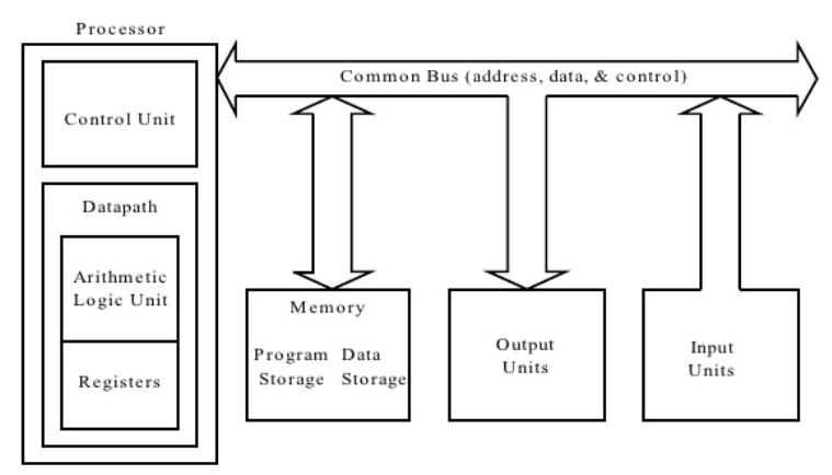
The bus is the data travel path between the cpu, dram and all other peripheral components. The CPU contains the registers, program counter and the arithmetic logic unit (ALU) that performs all the operations. The following figure depicts the overall structure with the peripheral devices.
总线是在中央处理器,内存和其它所有外围设备之间传输数据的通路。CPU 包括寄存器,程序计数器和算术逻辑单元(ALU)用于执行所有的操作。下图描述了带有外围设备的整体结构。
inst= mem[PC]
next_PC= PC+ 4

if ( inst.type== STORE) mem[rf[inst.arg1]] = rf[inst.arg2]
if ( inst.type== LOAD) rf[inst.arg1] = mem[rf[inst.arg2]]
if ( inst.type== ALU) rf[inst.arg1] = alu(inst.op, rf[inst.arg2], rf[inst.arg3])
if ( inst.type== COND) next_PC= rf[inst.arg1]

PC= next_PC
开始(Getting started)
Our emulator will have the following directory structure:
- riscv-emulator/
- src/
- includes/
- main.c
- Makefile
我们的模拟器包含以下目录结构:
- riscv-emulator/
- src/
- includes/
- main.c
- Makefile
The “includes” folder contains all the header files used, and the “src” directory contains all the source files corresponding to the headers. And we have our main.c file that binds everything together.
“includes” 文件夹包含所有用到的头文件,”src” 目录包含所有对应那些头文件的源文件。并且 main.c 文件是我们的主程序文件,它将模拟器的所有代码联系起来。
安装 riscv-gnu-toolchain (Installing the riscv-gnu-toolchain)
riscv-gnu-toolchain is the RISC-V C and C++ cross-compiler. It supports two build modes: a generic ELF/Newlib toolchain and a more sophisticated Linux-ELF/glibc toolchain.
riscv-gnu-toolchain 是 RISC-V C 与 C++ 的交叉编译器。它支持两种构建模式:一种是通用的 ELF/Newlib 工具链,另一种是更复杂的 Linux-ELF/glibc 工具链。
We will be using this compiler to compile programs written in C for the RISC-V isa, and generating the binaries for the written C programs for running on the emulator. To install the RISC-V gnu compiler, install the following prerequisites for your distro
我们将用这个编译器编译 C 语言编写的 RISC-V 指令集架构程序,并生成用于在模拟器中运行的二进制文件。要安装 RISC-V gnu 编译器,您的发行版需要先安装如下程序
autoconf automake curl python3 mpc mpfr gmp gawk base-devel bison flex texinfo gperf libtool patchutils bc zlib expat
And then run the following
之后执行如下代码
git clone https://github.com/riscv/riscv-gnu-toolchain
./configure --prefix=/opt/riscv
make && make linux
Now the compilers are located at
/opt/riscv/bin. If/opt/riscv/bin/is not in your environment PATH, add the directory to the PATH usingexport PATH=$PATH:/opt/riscv/bin/. Now we can compile C programs for the RISC-V platform using the following commands.(for the test file test.c)
现在编译器位于 /opt/riscv/bin。如果 /opt/riscv/bin/ 不在你的 PATH 环境变量中,你需要通过 export PATH=$PATH:/opt/riscv/bin/ 将其加入 PATH 中。现在我们就可以通过以下命令编译 RISC-V 平台的 C 语言程序了(测试文件名为 test.c)
# Generate assembly file test.s from test.c
# 根据 test.c 文件生成对应的汇编文件 test.s
riscv64-unknown-elf-gcc -S test.c
# Generate ELF executable test from test.s
# 根据 test.s 文件生成对应的 ELF 可执行文件 test
riscv64-unknown-elf-gcc -Wl,-Ttext=0x0 -nostdlib -march=rv64i -mabi=lp64 -o test test.s
# Generate binary file test.bin from ELF file test (what will be read by emulator)
# 根据 ELF 文件 test 生成二进制文件 test.bin (这是模拟器将要读取的文件)
riscv64-unknown-elf-objcopy -O binary test test.bin
使用 riscv-tests (Using riscv-tests)
RISC-V has a GitHub repository riscv-tests, which contains tests for every instruction for a riscv-core for various modules. We can check if our implementation of the RISC-V core works properly by running these tests. The tests for the different modules are located in the
isadirectory. Going over to the rsa directories, we can build the executables for the required modules, for example, if we want to test therv32uiwhich stands for rv32 userspace only integer instructions, simply run
RISC-V 有一个 GitHub 仓库 riscv-tests,其中包含用于 RISC-V 核心大部分模块每一条指令的测试。我们可以通过运行这些测试,来检测 RISC-V 核心的实现是否正确。用于不同模块的测试位于 isa 目录下。转到 rsa 目录下,我们可以为所需模块构建可执行文件。例如,当我们需要测试代表 rv32 仅限用户空间整数指令的 rv32ui 时,只需要执行
cd isa/
make rv32ui
We get all the RISC-V ELF executables and correspinding dump files containing the instructions executed. Now in our emulator, we read a binary file contents into the memory for execution. In order to convert the ELF executable to binary, we run the following
就可以得到所有 RISC-V ELF 可执行文件和对应的包含已执行指令的转储文件。现在在我们的模拟器中,我们可将二进制文件的内容读进内存用于执行。为了将 ELF 可执行文件转为二进制文件,我们执行以下命令:
riscv64-unknown-elf-objcopy -0 binary <filename> <filename>.bin
This will give us the required binary file for use with our emulator.
它将提供给我们模拟器执行所需的二进制文件。
编写 DRAM 结构体(Writing a DRAM struct)
The DRAM (Dyanmic random access memory) is our memory that contains all the instructions to be executed and the data. The memory for our emulator is simply an array of 64-bit variables, to store the 64-bit values. Here, we define the size of the memory by the variable
DRAM_SIZEand define the start address of the memory inDRAM_BASE. The memory has a start address higher than 0x0, because the RISC-V architecture has a memory mapped I/O.
DRAM(动态随机存取存储器)存放所有指令与数据。模拟器中的内存只是一个 64 位变量的数组,用于存放 64 位值。此处我们用变量 DRAM_SIZE 定义内存的大小,用变量 DRAM_BASE 定义内存的起始地址。内存有一个大于 0x0 的起始地址,因为 RISC-V 架构有一个内存映射 I/O。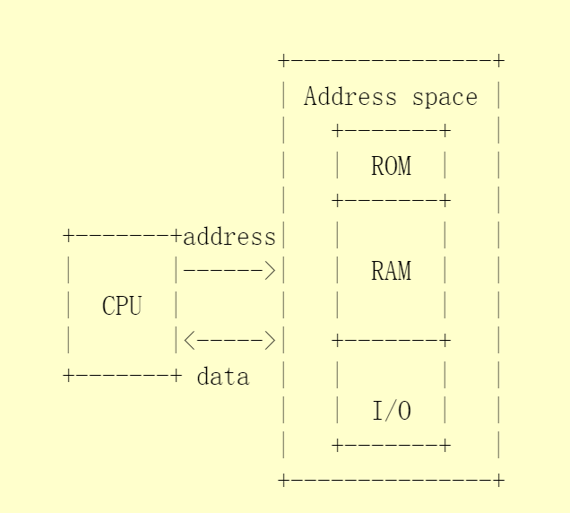
In memory mapped I/O, as shown in the above figure, the same address space is shared by both the memory and the I/O devices. In a QEMU VM, the lower addresses are used for I/O ports and the DRAM memory starts from the address 0x800000000. So, we use DRAM_BASE=0x80000000. Due to memory mapped I/O, we can perform I/O operations using any instruction that can reference memory. Otherwise, we would have needed seperate instructions and read/write bus for the I/O ports.
在内存映射 I/O 中,如上图所示,内存与 I/O 设备共享相同的地址空间。在 QEMU 虚拟机中,低地址用于 I/O 端口并且 DRAM 内存起始地址为 0x800000000。因此我们将 DRAM_BASE 的值定为 0x800000000。由于内存映射 I/O,我们可以使用任何能够访问内存的指令来执行 I/O 操作。否则,我们将需要单独的指令和 I/O 端口的读写总线。
So, we write our DRAM struct as follows.
因此,我们按如下代码编写 DRAM 结构
// includes/dram.h

#define DRAM_SIZE 1024*1024*1     // 1 MiB DRAM
#define DRAM_BASE 0x80000000

typedef struct DRAM {
    uint8_t mem[DRAM_SIZE];     // Dram memory of DRAM_SIZE
} DRAM;
The dram is the memory of the system. The CPU reads data and fetches instruction from the memory, and also stores/write data to the memory. So dram has two basic operations, reading from memory and writing from memory. These 2 functions are defined here as
dram_load()for reading anddram_store()for writing to the memory.
dram 是系统的内存。CPU 读取数据并从内存中取得指令,也向内存中存/写数据。因此 dram 有两个基本操作:从内存中读和写入内存。此处定义函数 dram_load() 用于读取内存以及 dram_store() 用于写入内存。
The
dram_load()takes the pointer to the dram to be read from, the address of the data to be read, and the size of the data to be read, which might be 8, 16, 32 or 64 bits, as per the instruction (LB, LH, LW, and LD respectively).
dram_load() 依据指令获取指向要读取的 dram 的指针,要读取的数据的地址,要读取的数据的大小。数据的大小可能是 8,16,32 或 64 位(分别对应 LB,LH,LW 和 LD)。
For simplicity, for each data size of read, seperate load functions are written, which will then be called from the main load function according to the given size. These are private functions and so not defined in the header, will be implemented in the src file. Thus, our load functions are:
为简单起见,对于要读取的每种大小的数据,编写单独的读取函数,然后根据给定的大小从主读取函数调用。这些函数是私有函数,因此不会在头文件中定义,而是在各自的源代码文件中实现。因此,我们有如下的读取函数:
// dram.h

uint64_t dram_load(DRAM* dram, uint64_t addr, uint64_t size);
Similar to the load functions, we also write store functions. The
dram_store(), takes the same args as the load functions, plus thevaluearg, which contains the data to be written to the given address of the given dram. Thus, our load functions are:
我们类似地编写写入函数。dram_store() 与读取函数拥有相同的参数,除此之外多了一个 value 参数,其表示要写入的数据。因此我们有如下的写入函数:
// dram.h

void dram_store(DRAM* dram, uint64_t addr, uint64_t size, uint64_t value);
DRAM 函数(DRAM functions)
dram_load() 与 dram_store()
This function takes a DRAM pointer, pointing to the DRAM to load data from, the address to load data from and the size of the data. Using a switch statement on the
sizeof the data to be load, dram_store_8() for 8 bits, and so on. The same goes for thedram_store()function.
函数传入一个指向要操作的 DRAM 的指针,要读取的地址与数据的大小。对要加载的数据的大小采用 switch 语句,对 8 位的数据调用 dram_load_8(),其余大小类似。这部分与 dram_store() 函数相同。
// dram.h
uint64_t dram_load(DRAM* dram, uint64_t addr, uint64_t size) {
    switch (size) {
        case 8:  return dram_load_8(dram, addr);  break;
        case 16: return dram_load_16(dram, addr); break;
        case 32: return dram_load_32(dram, addr); break;
        case 64: return dram_load_64(dram, addr); break;
        default: ;
    }
    return 1;
}
void dram_store(DRAM* dram, uint64_t addr, uint64_t size, uint64_t value) {
    switch (size) {
        case 8:  dram_store_8(dram, addr, value);  break;
        case 16: dram_store_16(dram, addr, value); break;
        case 32: dram_store_32(dram, addr, value); break;
        case 64: dram_store_64(dram, addr, value); break;
        default: ;
    }
}
Now, we write the functions to load specified number of bits, 8, 16, 32, and 64 from the DRAM. We note here that, due to use of memory mapped I/O, the address DRAM_BASE corresponds to the memory[0]. So, in order to access data at given
addr, we need to subtract DRAM_BASE from it. That is the start of the memory is atmem[addr-DRAM_BASE]
现在我们编写了用于读取特定位数 8,16,32,64 位数据的函数。注意到由于内存映射 I/O 的使用,地址 DRAM_BASE 对应的是 memory[0]。因此为了获取 addr 参数给定的地址上的数据,我们需要从 addr 中减去 DRAM_BASE。这意味着数据的实际起始地址为 mem[addr-DRAM_BASE]。
Also, the system we are building is a little endian system, since most systems today are little endian. Little-endian is an order in which the “little end” (least significant value in the sequence) is stored first, that is the least significant bytes are stored in the lower addresses. So while loading, we read the lower address values first into the bus by returning, and then, left shifting by 8 bits (1 byte) and AND with 0xff(8 1s) to get the lower byte only and clear all the higher bytes while ORing, load the next address into higher places, as per the required size. The implementation of
dram_load_32anddram_load_64are shown below. These functions should be defined before thedram_load()anddram_store()functions.
除此之外,我们正在构建的系统是一个用小端法表示数据的系统,因为现在的大多数系统都是小端法系统。小端法是将最小端(权值最低位)最先存储,即将最低字节存在最低地址的数据表示方法。当读取数据时,我们先读取最低的地址中存放的值通过返回值输送给总线,随后左移 8 位(1 字节)并与 0xff(8 个 1)进行与操作来得到最低字节的数据并清空高字节以便用于或操作,根据所读取数据的大小读取下一个地址的数据到更高位置。dram_load_32 和 dram_load_64 的实现如下所示。这些函数需要在 dram_load() 与 dram_store() 之前定义。
// dram.c
uint64_t dram_load_32(DRAM* dram, uint64_t addr){
    return (uint64_t) dram->mem[addr-DRAM_BASE]
        |  (uint64_t) dram->mem[addr-DRAM_BASE + 1] << 8
        |  (uint64_t) dram->mem[addr-DRAM_BASE + 2] << 16
        |  (uint64_t) dram->mem[addr-DRAM_BASE + 3] << 24;
}
uint64_t dram_load_64(DRAM* dram, uint64_t addr){
    return (uint64_t) dram->mem[addr-DRAM_BASE]
        |  (uint64_t) dram->mem[addr-DRAM_BASE + 1] << 8
        |  (uint64_t) dram->mem[addr-DRAM_BASE + 2] << 16
        |  (uint64_t) dram->mem[addr-DRAM_BASE + 3] << 24
        |  (uint64_t) dram->mem[addr-DRAM_BASE + 4] << 32
        |  (uint64_t) dram->mem[addr-DRAM_BASE + 5] << 40
        |  (uint64_t) dram->mem[addr-DRAM_BASE + 6] << 48
        |  (uint64_t) dram->mem[addr-DRAM_BASE + 7] << 56;
}
We write similar functions for the load_store functions. Since they write to the memory, they don’t return anything. And being little endian, we store the least significant byte first, then right shift by a byte to store the higher bytes.
dram_store_16anddram_store_64are shown below.
我们为 load_store 函数编写相似的函数。它们没有返回值,因为它们向内存中写入数据。并且由于小端法,我们首先存储最低字节,随后右移一字节以存储更高字节。dram_store_16 与 dram_store_64 如下所示。
// dram.c
void dram_store_16(DRAM* dram, uint64_t addr, uint64_t value) {
    dram->mem[addr-DRAM_BASE] = (uint8_t) (value & 0xff);
    dram->mem[addr-DRAM_BASE+1] = (uint8_t) ((value >> 8) & 0xff);
}
void dram_store_64(DRAM* dram, uint64_t addr, uint64_t value) {
    dram->mem[addr-DRAM_BASE] = (uint8_t) (value & 0xff);
    dram->mem[addr-DRAM_BASE + 1] = (uint8_t) ((value >> 8) & 0xff);
    dram->mem[addr-DRAM_BASE + 2] = (uint8_t) ((value >> 16) & 0xff);
    dram->mem[addr-DRAM_BASE + 3] = (uint8_t) ((value >> 24) & 0xff);
    dram->mem[addr-DRAM_BASE + 4] = (uint8_t) ((value >> 32) & 0xff);
    dram->mem[addr-DRAM_BASE + 5] = (uint8_t) ((value >> 40) & 0xff);
    dram->mem[addr-DRAM_BASE + 6] = (uint8_t) ((value >> 48) & 0xff);
    dram->mem[addr-DRAM_BASE + 7] = (uint8_t) ((value >> 56) & 0xff);
}
The full
dram.cfile can be found here
完整的 dram.c 文件见 此处
编写总线结构体(Writing a BUS struct)
A bus simply provides a path for data transfer across the various components of a computer. For our RISC-V emulator, the address bus and data bus is a single 64-bit wide bus (for 64 bit implementation). The bus, in our case, connects the CPU and the DRAM. So we write a BUS struct, with a DRAM object, to which it is connected to.
总线只是为计算机提供了一条各个组件之间数据传输的路径。对于我们的 RISC-V 模拟器,地址总线与数据总线是单一的 64 位宽总线(对于 64 位实现)。本例中的总线连接 CPU 与 DRAM。因此我们编写的总线结构有一个 DRAM 对象,表示我们要连接到的 DRAM。
// includes/bus.h

typedef struct BUS {
    struct DRAM dram;
} BUS;
We also define two functions
bus_load()andbus_store()which loads and stores values respectively to or from the provided address in the DRAM connected to the bus, a pointer to which is provided as function arg.
我们也定义了 bus_load() 与 bus_store() 函数,它们分别从总线连接到的 DRAM 中的给定地址上读取或写入数据。函数参数中有一个指针指向总线。
// includes/bus.h

uint64_t bus_load(BUS* bus, uint64_t addr, uint64_t size);
void bus_store(BUS* bus, uint64_t addr, uint64_t size, uint64_t value);
总线函数(BUS functions)
The bus functions simply load and store data from and to the dram using the public functions
dram_load()anddram_store()functions respectively. The functions are implemented as follows.
总线函数简单地用 dram_load() 与 dram_store() 的这两个公共函数从 dram 中存取数据。这两个函数的实现如下:
// bus.c
uint64_t bus_load(BUS* bus, uint64_t addr, uint64_t size) {
    return dram_load(&(bus->dram), addr, size);
}
void bus_store(BUS* bus, uint64_t addr, uint64_t size, uint64_t value) {
    dram_store(&(bus->dram), addr, size, value);
}
实现一个基本的 CPU 结构体(Writing a basic CPU struct)
Firstly, we write a CPU struct with all the components contained by the cpu,
- Registers: The RISC-V CPU has 32 registers each 64 bit wide (since we are implementing a 64 bit core). The register x0 is hardwired to 0, and the rest are used for storing values.
- There is another unprivileged register
pcwhich is the program counter. This register holds the address of the current instruction being executed.- And we have a
busthat connects our CPU to the system bus, for reading and writing data from and to the memory (DRAM) respectively.So, our CPU struct
CPUis written as follows. We write the struct definition in theincludes/cpu.hfile.
首先,我们要实现一个包含以下所有 CPU 组件的 CPU 结构。
- 寄存器:risc-v CPU 有 32 个寄存器,每个有 64 位宽(因为我们在实现一个 64 位的核心)。寄存器 x0 被硬连线到 0 值了,其它寄存器用于存放数据。
- 另一个非特权级寄存器是
pc,程序计数器。这个寄存器存放当前执行的指令的地址。 - 还包含一个
bus将我们的 CPU 连接到系统总线,用于从内存(DRAM)中读写数据。
因此,我们的 CPU 结构体 CPU 实现如下。这个结构体的定义在 includes/cpu.h 文件中。
// includes/cpu.h

#include <stdint.h>

typedef struct CPU {
    uint64_t regs[32];          // 32 64-bit registers (x0-x31)
    uint64_t pc;                // 64-bit program counter
    struct BUS bus;             // CPU connected to BUS
} CPU;
Having written the struct, we need to write functions for each of tasks of CPU pipeline. We define the following functions
实现这个结构体后,我们需要编写 CPU 流水线上每一段的函数。我们定义如下函数:
// includes/cpu.h

void cpu_init(struct CPU *cpu);
uint32_t cpu_fetch(struct CPU *cpu);
int cpu_execute(struct CPU *cpu, uint32_t inst);
void dump_registers(struct CPU *cpu);
- The
cpu_initfunction initializes the provided CPU by pointer by 0 initializing all the 32 registers, and setting the program counterpcto the start of the memory.- The
cpu_fetchfunction reads instructions from the memory (DRAM) for execution, and stores it to the instruction variableinst.cpu_executeis basically the ALU and the instruction decoder combined. It decodes the instruction fetched from the DRAM in theinstvariable and executes the instruction accordingly.dump_registeris just a debug function to view the contents of the 32 registers when needed.
cpu_init函数初始化给定的 CPU,将指针指向的 CPU 中的寄存器全部置 0,并将程序寄存器pc的值设为内存的起始地址。cpu_fetch函数从内存(DRAM)中读取指令用于执行,并将其存入指令变量inst中。cpu_execute基本上是 ALU 和指令译码器的组合。它将从 DRAM 中取得并存放在inst变量中的指令解码并执行。dump_register只是调试函数,用于在需要时查看寄存器的值。
CPU 函数(CPU Functions)
Now, we write the CPU functions as defined in the header file in the file
src/cpu.c.
现在,我们编写在头文件 src/cpu.h 中定义的头文件。
cpu_init()
First, we write the
cpu_initfunction. This function zero initializes all the 32 64-bit registers. The register x02, contains the stack pointer SP, which should point to the top of the memory. So x02 should be equal to the the DRAM_SIZE plus the base address from which the memory starts, DRAM_BASE. So, x02=DRAM_SIZE+DRAM_BASE. And finally, the program counter should point to the start of the memory which contains the first instruction. So, pc=DRAM_BASE.
首先实现 cpu_init() 函数。该函数将全部 32 个 64 位寄存器初始化为 0。寄存器 x02 存放着栈指针 SP,它指向内存的顶部。因此 x02 应该等于 DRAM_SIZE 加上内存开始位置,也就是加上基地址 DRAM_BASE。于是 x02=DRAM_SIZE+DRAM_BASE。最后,程序计数器应该指向内存起始位置,即第一条指令所在处。因此,pc=DRAM_BASE。
// cpu.c

 void cpu_init(CPU *cpu) {
     cpu->regs[0] = 0x00;                    // register x0 hardwired to 0
     cpu->regs[2] = DRAM_BASE + DRAM_SIZE;   // Set stack pointer
     cpu->pc      = DRAM_BASE;               // Set program counter to the base address
 }
cpu_fetch()
Now, we write the
cpu_fetch(). This instruction fetches the instruction data at the program counter address from the dram. The data is put on the bus from the dram using thedram_load()function where we load the data at the address given by thepcwhich points to the instruction to be read. So our function can be written as follows.
现在我们编写 cpu_fetch()。它从 dram 中按照程序计数器所存储的地址获取指令数据。通过 dram_load() 函数读取 pc 指向的地址上的数据,并将其放进总线。该函数实现如下:
// cpu.c
uint32_t cpu_fetch(CPU *cpu) {
    uint32_t inst = bus_load(&(cpu->bus), cpu->pc, 32);
    return inst;
}
私有读写函数(Private load/store functions)
We write two private functions
cpu_load()andcpu_store()functions for loading and storing data. These functions just use the bus load/store functions to read/write data from/to the dram.
我们实现两个函数 cpu_load() 与 cpu_store() 用于装载与存储数据。这些函数用总线读写函数来从 dram 中获取数据,或是写入 dram。
uint64_t cpu_load(CPU* cpu, uint64_t addr, uint64_t size) {
    return bus_load(&(cpu->bus), addr, size);
}

void cpu_store(CPU* cpu, uint64_t addr, uint64_t size, uint64_t value) {
    bus_store(&(cpu->bus), addr, size, value);
}
指令译码(Instruction decoding)
The instruction that we read from the dram for executeion is 32-bit wide. These 32 bits contain all the directives for the operation to perform, like the opcode which defines the operation to perform, the source and destination registers to read/write from/to, the immediate value and so on. The decoding will be different for different types of instructions which are categorized into the following:
- R-Type: Register type instructions
- I-Type: Immediate type instructions
- S-Type: Store type instructions
- B-Type: Break type instructions
- U-Type: Register type instructions
- J-Type: Jump type instructions
从 dram 中读取的用于执行的指令是 32 位宽的。这 32 位包含所有要执行的操作对应的指令,比如操作码,用于读/写的源寄存器和目标寄存器,立即数值等等。对于不同类型的指令的译码是不同的,指令类型有以下几种:
- R 类型:寄存器类型指令
- I 类型:立即数类型指令
- S 类型:存储类型指令
- B 类型:中断类型指令
- U 类型:寄存器类型指令
- J 类型:跳转类型指令
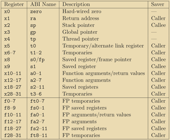
The following table shows the map for the registers for the different types of instructions.
下表展示了不同类型指令的寄存器的映射关系。
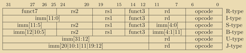
Here, the annontations are:
opcode
Lower 7 bit (inst[6:0]) specifies the code for each CPU operation
rd
A 4 bit value (inst[11:7]) which gives the address of destination register
funct3
A 3 bit value (inst[14:12]). The opcode is the same for a group of similar category operations e.g. (ADD, SUB, DIV, MUL, etc.). In such cases, the group can contain upto 8 different instructions for 8 values of funct3.
funct7
A 7 bit value (inst[31:25]). Just like funct3, funct7 divides a group of same funct3 instructions into multiple instructions. For example, SR(shift right) has 2 instuctions: SRA (arithmetic shift) and SRL (logical shift) for different funct7
rs1
A 4 bit value (inst[19:15]) which gives the address of source register 1
rs2
A 4 bit value (inst[24:20]) which gives the address of source register 2
imm
A value which gives the address of destination register
shamt
shamt is located in the lower bits of imm and stores the shift amount for shift instructions
注释如下:
opcode
低 7 位(inst[6:0])用于区别每个 CPU 操作
rd
一个 4 位值(inst[11:7]),给定目标寄存器的地址。
funct3
一个 3 位值(inst[14:12]),每一组类似操作的操作码相同(如 ADD,SUB,DIV,MUL 等等)。每组可包括至多 8 个不同指令,对应 8 个不同的 funct3 值。
funct7
一个 7 位值(inst[31:25])。与 funct3 类似,funct7 将一组相同的 funct3 指令划分为多个指令。例如,SR(右移)有两个指令:SRA(算数右移)与 SRL(逻辑右移)对应不同的 funct7。
rs1
一个 4 位值(inst[19:15]),给定源寄存器 1 的地址。
rs2
一个 4 位值(inst[24:20]),给定源寄存器 2 的地址。
imm
原文为“一个用于表示目标寄存器的地址的值”,有误。此处 imm 应表示立即数。
shamt
shamt 位于 imm 的低位,存有移位指令的移位量。
We write functions for decoding each part of the 32 bit instruction mentioned above. The decoding structure varies according to the different types of instruction. The one that we need to take care of in such case is the
imm, which is the immediate value. The rest of the blocks can be decoded using a common function for all the five blocks. Following the instruction map given above, we write the following functions for decoding each block. Necessary comments have been added to understand the positioning of the blocks in the instruction.
我们为 32 位指令的上述每一部分编写译码函数。译码结构根据指令类型有所不同。尤其需要注意的是 imm,其对应的是立即数值。其余区块可以用通用的译码函数。按照上面给定的指令映射图,我们编写如下的函数用于译码每一个区块。为了使每个区块在指令中的位置更易理解,代码中已经添加了必要的注释。
// cpu.c
uint64_t rd(uint32_t inst) {
    return (inst >> 7) & 0x1f;    // rd in bits 11..7
}
uint64_t rs1(uint32_t inst) {
    return (inst >> 15) & 0x1f;   // rs1 in bits 19..15
}
uint64_t rs2(uint32_t inst) {
    return (inst >> 20) & 0x1f;   // rs2 in bits 24..20
}
uint64_t imm_I(uint32_t inst) {
    // imm[11:0] = inst[31:20]
    return ((int64_t)(int32_t) (inst & 0xfff00000)) >> 20;
}
uint64_t imm_S(uint32_t inst) {
    // imm[11:5] = inst[31:25], imm[4:0] = inst[11:7]
    return ((int64_t)(int32_t)(inst & 0xfe000000) >> 20)
        | ((inst >> 7) & 0x1f);
}
uint64_t imm_B(uint32_t inst) {
    // imm[12|10:5|4:1|11] = inst[31|30:25|11:8|7]
    return ((int64_t)(int32_t)(inst & 0x80000000) >> 19)
        | ((inst & 0x80) << 4) // imm[11]
        | ((inst >> 20) & 0x7e0) // imm[10:5]
        | ((inst >> 7) & 0x1e); // imm[4:1]
}
uint64_t imm_U(uint32_t inst) {
    // imm[31:12] = inst[31:12]
    return (int64_t)(int32_t)(inst & 0xfffff999);
}
uint64_t imm_J(uint32_t inst) {
    // imm[20|10:1|11|19:12] = inst[31|30:21|20|19:12]
    return (uint64_t)((int64_t)(int32_t)(inst & 0x80000000) >> 11)
        | (inst & 0xff000) // imm[19:12]
        | ((inst >> 9) & 0x800) // imm[11]
        | ((inst >> 20) & 0x7fe); // imm[10:1]
}
uint32_t shamt(uint32_t inst) {
    // shamt(shift amount) only required for immediate shift instructions
    // shamt[4:5] = imm[5:0]
    return (uint32_t) (imm_I(inst) & 0x1f); // TODO: 0x1f / 0x3f ?
}
cpu_execute()
Now that we have decoded our instruction, we can execute the instructions as per the decoded data. The opcodes tell us what operation to perform with the provided data and registers. What exact operation we should perform, depends on 3 values, the opcode, funct3 and funct6. As per the map of the instruction, we decode these 3 using the following in the
cpu_executefunction.
现在我们已经将指令译码,我们可以根据译码后的数据执行指令。操作码告诉我们要对给定的地址和寄存器进行什么操作。具体要进行什么操作取决于 3 个值:操作码 opcode,funct3 和 funct7(此处原文笔误写成了 funct6)。根据指令映射,我们用以下 cpu_execute 函数对这 3 个部分进行译码。
// cpu.c

int cpu_execute(CPU *cpu, uint32_t inst) {
    int opcode = inst & 0x7f;           // opcode in bits 6..0
    int funct3 = (inst >> 12) & 0x7;    // funct3 in bits 14..12
    int funct7 = (inst >> 25) & 0x7f;   // funct7 in bits 31..25

    cpu->regs[0] = 0;                   // x0 hardwired to 0 at each cycle
Here, since the register x0 is hardwired to 0, we have to manually set it to 0 at each CPU cycle, since the emualtor does not have any real 0 (GND) to tie to.
此处由于寄存器 x0 是硬件 0,我们必须在每一个 CPU 周期之后手动将其置为 0,因为模拟器没有真正的 0(GND)可以用来绑定。
Now, that we have our opcode, we can start executing instructions accrodingly. The instruction set table for the different modules are given in the RISC-V specifications book. According to the table, we check our opcodes using a switch to find which operation to perform and execute that operation on the given resiters or immediates. For example, the table for the simple arithmetic and logical oprations like ADDI, ORI, ANDI, which operates with the given immediate value is:
现在我们有了操作码,可以开始根据操作码执行指令。不同模块的指令集表格已经在 RISC-V 规范中给出。根据表格,我们可以用 switch 语句来确定要执行何种操作并在给定的寄存器或立即数上执行操作。例如,使用给定的立即数值进行简单算术与逻辑操作的指令如 ADDI,ORI,ANDI 的表格如下所示:

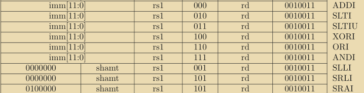
Here, we see, the opcode for these I-Type instructions are 0010011. Now dealing with such binaries for the case statements makes the code un-understandable. So, we define the opcodes and the respective operation names in an
opocodes.hfile in our “includes/” folder. For the I-type instructions, we can define the opcodes as follows using the hex codes of the given binaries.
从这我们能够看见,I 型指令的操作码是 0010011,用 case 语句处理类似的二进制串会使得代码变得难以理解。因此,我们在 “includes/” 文件夹下的 opcodes.h 文件中定义操作码对应的名称的宏。对于 I 型指令,我们可以使用十六进制数代替二进制字符串,来定义如下宏。
// opcodes.h
#define I_TYPE  0x13
    #define ADDI    0x0
    #define SLLI    0x1
    #define SLTI    0x2
    #define SLTIU   0x3
    #define XORI    0x4
    #define SRI     0x5
        #define SRLI    0x00
        #define SRAI    0x20
    #define ORI     0x6
    #define ANDI    0x7
Here, we see, for the same opcode
0x13we have different operations based onfunct3. Again, for the same funct30x5we have two operations as per different values offunct7.
在这里,我们看到,对于相同的操作码 0x13,我们根据 funct3 定义不同的操作。同样,对于相同的 funct3 0x5,我们根据 funct7 的不同值定义了两个操作。
Now, for these I-Type instructions, we can write our switch statement as follows.
现在,对于 I 型指令,我们可以写出如下语句
// cpu.c

switch (opcode) {
    case I_TYPE:
        switch (funct3) {
            case ADDI:  exec_ADDI(cpu, inst); break;
            case SLLI:  exec_SLLI(cpu, inst); break;
            case SLTI:  exec_SLTI(cpu, inst); break;
            case SLTIU: exec_SLTIU(cpu, inst); break;
            case XORI:  exec_XORI(cpu, inst); break;
            case SRI:
                switch (funct7) {
                    case SRLI:  exec_SRLI(cpu, inst); break;
                    case SRAI:  exec_SRAI(cpu, inst); break;
                    default: ;
                } break;
            case ORI:   exec_ORI(cpu, inst); break;
            case ANDI:  exec_ANDI(cpu, inst); break;
            default: ;
        } break;

    default:
        fprintf(stderr,
                "[-] ERROR-> opcode:0x%x, funct3:0x%x, funct3:0x%x\n"
                , opcode, funct3, funct7);
        return 0;
        /* exit(1); */
}
For each of the operations, we will be writing a
exec_<op-name>function which takes the CPU pointer and the instruction as args.对于每一个操作,我们会写一个名为
exec_<op-name>的函数,其拥有 CPU 指针和指令作为参数。
Here, in case we have a wrong opcode, or if the operation is not implmented yet, we print to stderr with the opcode that failed as defalut.
此处为了防止我们编写错误的操作码,或是操作尚未被实现,我们将失败的操作码作为默认值打印到 stderr。
Now, we write the
execfunctions for each of the operations. What each operation does has been well explained in the RISC-V specs. The executions were written following those.
现在,我们为每个操作编写 exec 函数。RISC-V 规范中已经解释了每一个操作具体该做什么,执行函数是根据那些编写的。
While writing the exec functions, care should be taken regarding which parts will be sign extended or zero extended. For example, imm is often sign-extended to 64-bits before being operated on with other values in registers. We can sign extend in C by typecasting by the serial (int32_t) > (int64_t) > (uint_64t), when needed.
当编写 exec 函数时,应当注意 0 扩展与符号扩展。例如,立即数在与寄存器中的其它值一起被操作时,通常是符号扩展到 64 位。我们可以在需要时通过 C 语言的类型转换(int32_t) > (int64_t) > (uint64_t) 来实现符号位扩展。
// cpu.c
void exec_ADDI(CPU* cpu, uint32_t inst) {
    uint64_t imm = imm_I(inst);
    cpu->regs[rd(inst)] = cpu->regs[rs1(inst)] + (int64_t) imm;
    print_op("addi\n");
}
void exec_SLTI(CPU* cpu, uint32_t inst) {
    uint64_t imm = imm_I(inst);
    cpu->regs[rd(inst)] = (cpu->regs[rs1(inst)] < (int64_t) imm)?1:0;
    print_op("slti\n");
}
void exec_SRAI(CPU* cpu, uint32_t inst) {
    uint64_t imm = imm_I(inst);
    cpu->regs[rd(inst)] = (int32_t)cpu->regs[rs1(inst)] >> imm;
    print_op("srai\n");
}
Following the RISC-V specs book, we write down all the rest of the opcodes in the
opcodes.hfile, include their cases in the switch statement and write their execution functions. All of the operations are pretty basic and easy to get. The ones I had some difficutly understanding are:
根据 RISC-V 规范,我们在 opcodes.h 文件中实现剩余的操作码,将这些操作码添加到 switch 语句的 case 中,并编写它们的执行函数。所有的操作都很基本而且容易理解。一些我感到稍微难以理解的是:
LUI
AUIPC
main 文件(The main file)
Now, we connect all the structs and functions written in the
main.cfile, which will run our emulator loop, taking the binary file as the input.
现在,我们将所有的结构体与函数通过 main.c 文件连接在一起,它将会运行我们的模拟器循环,将二进制文件作为输入。
Firstly, we need to read the contents of the input binary file into the memory. The filename for the binary file is taken input as a command line arg. Then, in order to read the contents of the file byte by byte, we write the following
read_filefunction, which takes thecpuand the provided binaryfilenameas args. The function reads the binary contents of the file, and writes them to the DRAM memory of the provided CPU pointer.
首先,我们需要将二进制文件中的内容读入内存。二进制文件的文件名以命令行参数的形式输入。随后,为了逐字节读入内容,我们编写 read_file 函数,它会将 cpu 与给定的二进制文件名 filename 作为参数。这个函数读入二进制文件的内容,并将其写入给定的 CPU 指针指向的 CPU 的 DRAM 中。
// main.c

void read_file(CPU* cpu, char *filename)
{
    FILE *file;
    uint8_t *buffer;
    unsigned long fileLen;

    //Open file
    file = fopen(filename, "rb");
    if (!file) {
        fprintf(stderr, "Unable to open file %s", filename);
    }
    //Get file length
    fseek(file, 0, SEEK_END);
    fileLen=ftell(file);
    fseek(file, 0, SEEK_SET);

    //Allocate memory
    buffer=(uint8_t *)malloc(fileLen+1);
    if (!buffer) {
        fprintf(stderr, "Memory error!");
        fclose(file);
    }
    //Read file contents into buffer
    fread(buffer, fileLen, 1, file);
    fclose(file);
    // Print file contents in hex
    for (int i=0; i<fileLen; i+=2) {
        if (i%16==0) printf("\n%.8x: ", i);
        printf("%02x%02x ", *(buffer+i), *(buffer+i+1));
    }
    printf("\n");

    // copy the bin executable to dram
    memcpy(cpu->bus.dram.mem, buffer, fileLen*sizeof(uint8_t));
    free(buffer);
}
Now, we write the main function. First we create a new CPU of type struct
CPU. We initialize the CPU usingcpu_init(), then use theread_file()function to read the contents of the binary file to the DRAM memory.
现在我们写完了主函数。首先我们创建一个 CPU 结构体类型的新对象 CPU。通过 cpu_init() 函数初始化这个 CPU。随后使用 read_file() 函数将二进制文件的内容读入 DRAM 内存。
The next part performs the CPU fetch and execution loop. In this implementation, we have a 3 stage instruction pipeline to execute all the instructions. These are:
- Stage 1 (fetch Instruction): Here, the CPU reads the instruction from the address (stored in the program counter pc) of the DRAM.
- Stage 2 (Instruction Decode): Here, the fetched instruction is decoded to get the opcode, destination and source registers, etc.
- Stage 3 (Instruction Execute): Here, the instruction is executed following the decoded bits, in the ALU.
下一部分执行 CPU 取指与执行循环。在这个实现中,我们有 3 级流水线用于执行所有指令,它们是:
- 第 1 级流水线(取指):cpu 从 DRAM 的特定地址(存放在程序计数器 pc 中)中取得指令
- 第 2 级流水线(译码):指令被译码为操作码,目标寄存器与源寄存器等。
- 第 3 级流水线(执行):此时指令按照译码后的结果在 ALU 中执行。
The stage 1 is handled by the
cpu_fetch()function and the stages 2 and 3 are handled together in thecpu_execute()function defined in thecpu.hfile. The program counter, pc, is incremented by 4 bytes(32 bits, since each instruction is 32 bit wide for riscv) at each loop, to get the next instruction from the memory. Thus our CPU processing loop can be written as follows.
第 1 级流水线由函数 cpu_fetch() 处理。第 2、3 级流水线由定义在 cpu.h 中的函数 cpu_execute() 一并处理。程序计数器 pc 在每次循环后增加 4 个字节(32 位,因为每个 RISC-V 指令长度都为 32 位),以获取下一条指令。因此 CPU 执行循环可以被写为下面这样:
// main.c

// Initialize cpu, registers and program counter
struct CPU cpu;
cpu_init(&cpu);
// Read input file
read_file(&cpu, argv[1]);

// cpu loop
while (1) {
    // fetch
    uint32_t inst = cpu_fetch(&cpu);
    // Increment the program counter
    cpu.pc += 4;
    // execute
    if (!cpu_execute(&cpu, inst))
        break;
    dump_registers(&cpu);
    if(cpu.pc==0)
        break;
}
return 0;
}
猜你喜欢:
- 我要投稿:发表原创技术文章,收获福利、挚友与行业影响力
- 知识星球:独家 Linux 实战经验与技巧,订阅「Linux知识星球」
- 视频频道:泰晓学院,B 站,发布各类 Linux 视频课
- 开源小店:欢迎光临泰晓科技自营店,购物支持泰晓原创
- 技术交流:Linux 用户技术交流微信群,联系微信号:tinylab
| 支付宝打赏 ¥9.68元 | 微信打赏 ¥9.68元 | |
 |  请作者喝杯咖啡吧 |  |
Read Album:
- Stratovirt 的 RISC-V 虚拟化支持(六):PLIC 和 串口支持
- Stratovirt 的 RISC-V 虚拟化支持(五):BootLoader 和设备树
- Stratovirt 的 RISC-V 虚拟化支持(四):内存模型和 CPU 模型
- Stratovirt 的 RISC-V 虚拟化支持(三):KVM 模型
- Stratovirt 的 RISC-V 虚拟化支持(二):库的 RISC-V 适配